 |
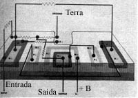
| Fig. 280 - schematics showing
a wide-band video amplifier manufactured circa 1962
using the passive thin-film techniques composed
of 3 transistors, 2 zener diodes, and 6 resistors.
With this technique all active elements can build
on a single semiconductor substrate and interconnected
with passive elements on a passive substrate |
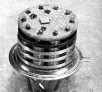 |
| Fig. 279 -Close up showing the
four separate circuit layers capable of housing
four isolated circuits with the equivalent of up
to one hundred separate components |
 |
| Fig. 281a - Modern integrated
circuit plastic case drilled to show the die inside
and its pin connections. |
 |
| Fig. 281d - Pure Silicon. Silicon
is common used for the manufacturing of FET transitors,
integrated circuits and so forth. However, nowadays
others alternatives have been found in compound
semiconductor materials such as: Gallium Arsenide,
Indium Phosphide, and Mercury Cadmium Telluride,
Cadmium Sulphide and Cadmium Telluride. |
|
 |
| Fig. 281b - the structure of a modern
integrated circuit observed through a microscope using
the Nomarsky interference constrat technique. |
 |
| Fig. 281 - Several types of modern semiconductor
devices: a) Transistor b) Transistor c) Integrated circuit
|
In 1952, during a conference in the USA, the Bristish scientist
Geoffre y William Arnold Dummer, considering the advent of the
transistor and the present status of the semicondutor technology
stated it would be possible to envisage electronic equipment
made in a solid block with no connecting wires. In this way,
the block may consist of layers of insulating, conducting, rectifying
and amplifying materials, whose electrical functions would be
connected directly by cutting out areas of the various layers.
Such increadible prophetic soon became a reality as two engineers,
Jack Kilby and Robert Noyce, working independently credited
in 1959 with the invention of the first integrated circuits.
In 1958, Jack Kilby working in the microminiaturization laboratory
at Texas Instruments Company had applied for his patent of the
first reliable integrated circuit. His researche was based in
the feasibility to fabricate resistors, capacitors and transistor
from semiconductor material. While resistors could make use
of the ohmic properties of bulk material, reverse-biased pn
junctions formed the capacitors. In the design of this first
flip flop circuit it was built simultaneously in a block of
monolithic Germanium the bulk resistors, pn junction capacitors,
and the Mesa transistors, using the photoetching techniques.
Therefore, this type of integrate circuit had some shortcomings
such as: - The performance of the individual components in the
circuit could not be optimized. - The interconnection of devices
made it diffficult to manufature the circuit, and finally, -
Its designs were expensive and difficult to be modified. However
in 1959, the aforementioned disadvantages were soon overcamed
through a new process developed by Robert Noyce, manager of
the research and development laboratories of the semiconductor
division at Fairchild, based in the transistor planar technology.
In this way just after the concept proposed by Noyce, by evaporating
metal onto the surface made the interconnecting, a patent was
applied for starting soon the manufacturing stage, where the
resitors and transitors were made by difusion in a slab of of
Silicon. Fig 279
 |
| Fig. 282 - a modern integrated circuit. |
In fact in the early days of integrated circuit development,
the same were first built in convetional way, using discrete
components to make sure they would function properly, before
rendered in integrate circuit form. In this way, every junction
and a connection has its counterpart in the integrated circuit.
Therefore, the integrate circuit performed in terms of building
blocks, whose integrated circuitry functions were controlled
by gates or a bistable latch as know as a flip-flop, or digital
memomories controled by a clock pulse and in this way giving
birth to an operational logic. The first integrated circuits
made by Fairchild used the RTL logic or - resistor-transistor
logic and were marked as a component family under the trade
name "Micrologic" The mass production of integrated circuits
started in 1960. At the beginning besides high price tag they
still had some operational drawbacks due to the different
types of coupling techniques used between the transistors
stages. Fig 280 In early sixties, Pacific Semiconductor Company
launched in the market the TTL logic or Transitor-Transistor
Logic, as well as through the researches of the IC designer
James L. Buie had devised a better coupling technique known
as transistor-coupled transitor logic - TCTL. Fig. 281 Even
though the great evolution in the integrated circuits manufacturing,
the same still used bipolar transitors as the backbone of
their circuit layout. Fig. 282 Therefore, the bipolar transistor
still had a high production cost as well as it was technically
too limited for the complexity of the new integrated circuit
topology. Soon the MOS technology developed from the researches
started with the field effect transitor - MOSFET - was used
in the production of semiconductor devices with high integration
capacity in such way in a small area it was possible to incorporate
a higher number of gates. Fig 283
| |
Fig.
281 c - The silicon wafer prepared from the pure Silicon.
Wafer or a precise semicondutor material substrate should
be carefully prepared in several stages such as: slicing
from the crystal and then precisely lapped and polished
to obtein a scratch free surface with tight flatness
and thickness tolerances. Wafer thinning, often known
as backlapping, is generally carried out at the end
of the manufacture process in order to reduce wafer's
thermal conductivity and to speed up signal transmission
across the device. Generally this involves reducing
the wafer thickness from initial 400-500 mm to between
100 to 150 mm. Nowadays due to increasingly sophisticated
semiconductor devices are demanding thinner wafers around
50 mm or less. |
Microprocessors
Introduced in 1971, the
miniature electronic devices, which could handle several
logical processing functions as know as LSI microprocessors
– large scale integration –, which led
to the fantastic computer
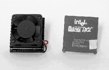 |
| The Intel™ microprocessor
486DX 2™ provided with the cooler. |
revolution. The first microprocessors
were built in Silicon chips and originally were used
in calculators’ machines. In 1974 the American
company “Intel™” developed the 8080™
microprocessor, which was used to manufacturer the
first personal computer. Since then the company launched
a family of microprocessors, among them the most important
landmarks are:
Type 80286™: as known as 286™, which as
manufactured and distributed in large quantities all
over the world.
Type 386™: the revolutionary microprocessor
was built in 32 Bits chip that could run multiple
programs at the same time.
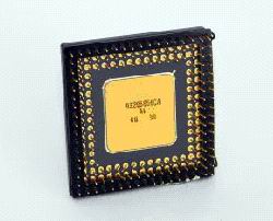 |
| The Intel™ microprocessor
486 DX2™ provided with 168-pin grid. |
Type 486™: it was
the first miniature electronic device to offer a built-in
mathematical coprocessor which speeded up computing
as well as allowing easier installation of hardware
with plug and play Bios and greater speed. In the
photograph it is shown the microprocessor 486 DX2™
provided with 168 pin grid array supported by 5V CC
and the cooler; it was replaced soon by the faster
type 486 DX4™.
Type Pentium™: originally it was the microprocessor
type 586™, launched in the market in 1993. This
was big leap when compared with the predecessor type
486™ as it was designed to include speech, sound
and photographic images. Initially Pentium chip arose
several difficulties such as high price as well as
technical handicaps; among them the overheating which
was quickly solved by placing a fan over the chip.
This new family of microprocessors comprises the types
Pentium Pro™, II, III and the latest IV.
|
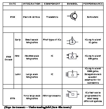
| Fig. 283 - Table showing the evolution
of semiconductor devices: from the transistor to microprocessors. |
 |
|